The Modulo ADC
In practice, a printed circuit board (PCB) is designed to perform the modulo operation in the analog domain. The modulo operation is defined as:
The implementation of the Modulo ADC (MADC) can be tailored to specific applications, with the design optimized for different input frequency and amplitude ranges. Here, we introduce a low-cost (approximately $20) and easy-to-build MADC architecture. This design features an integrator-based Modulo Analog-to-Digital Converter, as proposed in [12].
MADC Implementation
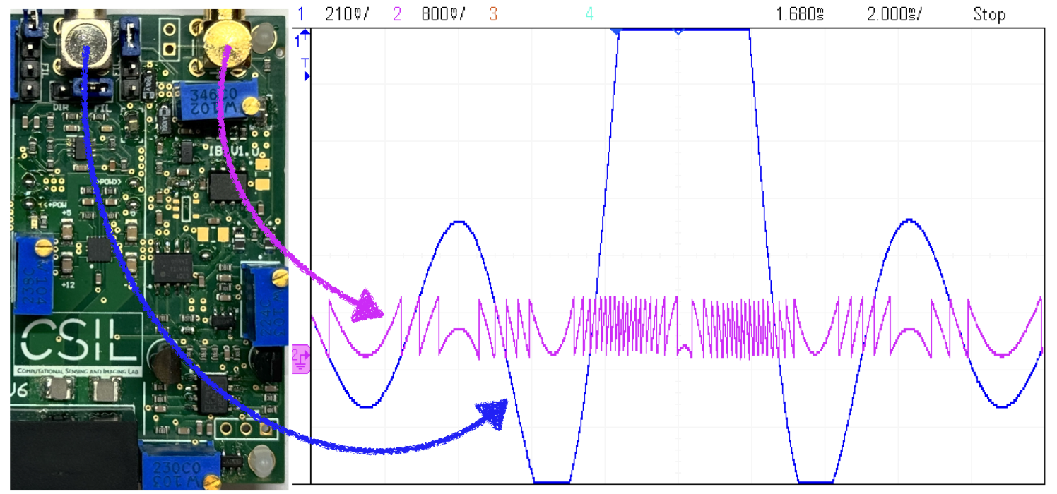
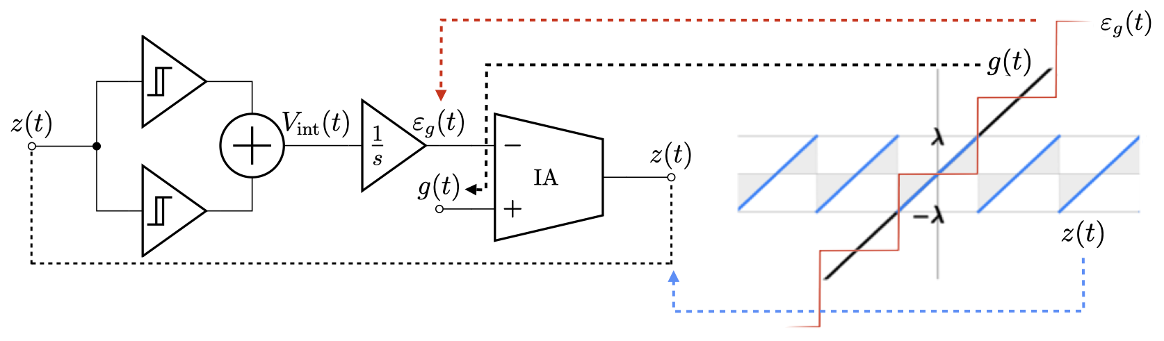
The overall system structure is illustrated in the block diagram below, with its resulting transfer function shown on the right. Let \(g(t)\) represent the input signal and \(z(t)\) be the output of the modulo function \(\MO\). The operation is carried out by three main blocks: the subtractor, the integrator, and a pair of Schmitt triggers.
The Subtractor
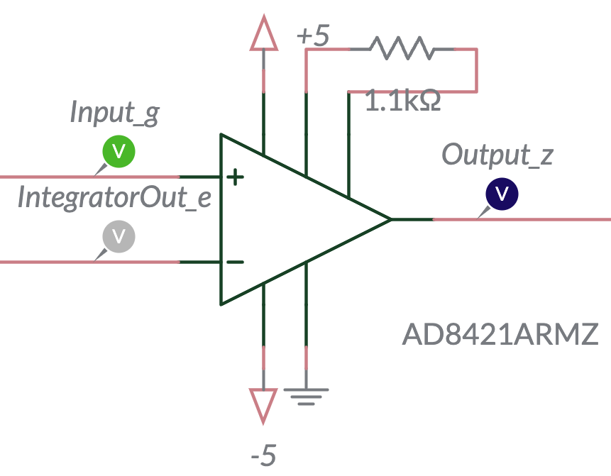
An auxiliary function \(\varepsilon_g(t)\) can be defined to help derive the modulo output \(z(t)\), as illustrated in the transfer diagram above. The subtraction can easily be carried out using an instrumentation amplifier (IA). Additionally, the adjustable gain of the IA provides a unique boost in performance to the system that will be explained later.
\[z(t) = g(t) - \varepsilon_g(t)\]
|
|
The Integrator
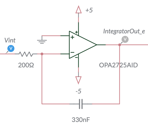
The auxiliary function \(\varepsilon_g(t)\) is generated by an integrator. The output of an operational amplifier (op-amp) integrator with an input signal \(V_{\texttt{int}}(t)\) is given by the following equation and is illustrated below.
\[\varepsilon_g(t) = -\frac{1}{RC} \int_{0}^{t} V_{\texttt{int}}(\tau) \, d\tau + \varepsilon_g(0)\]
|
|
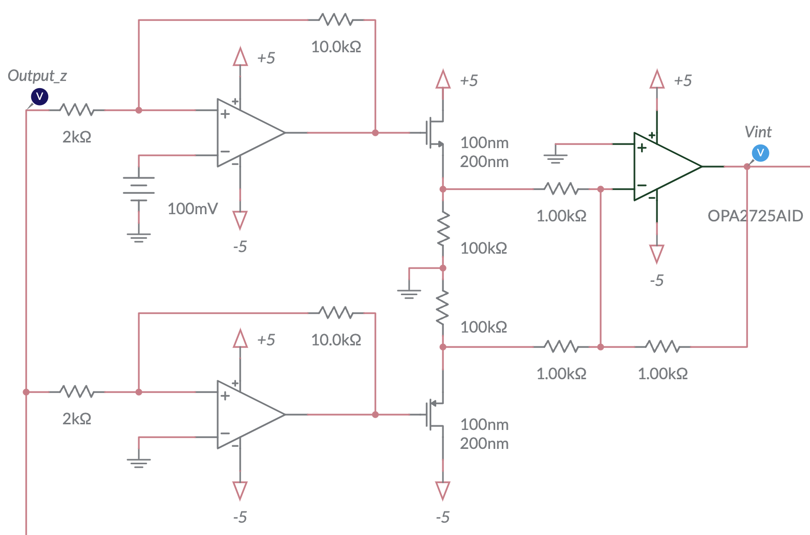
The Comparators with Hysteresis
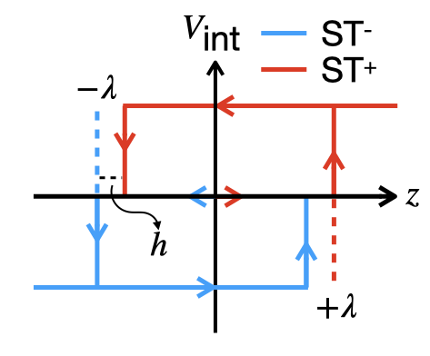
The integrator input \(V_{\texttt{int}}(t)\) is a composite signal formed from a pair of Schmitt triggers (STs) that take the modulo output \(z(t)\) as input. The transfer function of the system and a circuit to realize this setup are shown below.
|
|
The Folding Process
The folding process is initiated by the pair of STs. Whenever \(|z(t)| > \lambda\), \(\text{ST}^{+}\) (shown in red) generates a positive voltage, while \(\text{ST}^{-}\) (shown in blue) remains at 0 V. The combined output of the STs causes the integrator output \(\varepsilon_g(t)\) to increase sharply, thereby driving the modulo output \(z(t)\) downwards.
Once \(z(t)\) drops below \(h - \lambda\), \(\text{ST}^{+}\) resets to 0 V, stabilizing the integrator at a constant voltage and completing the folding cycle. The hysteresis parameter \(h\) is manually adjusted, as suggested in [6], to prevent unwanted oscillations and erratic jumps.
The Online Playground
Here is an interactive schematic of the MADC system.
For users who cannot view the iframe, click here to access the schematic directly.