In chapters 4 and 5, it was shown that the spectra of waveforms by AFM and DFM could be computed and the harmonics determined. In chapter 6, we discussed the characteristics of a waveform envelope. In order to demonstrate the feasibility of both AFM and DFM in real-time digital music synthesis, the real-time generation of musical sounds using both techniques was undertaken using a fast and modern digital signal processing (DSP) chip to process the AFM and DFM algorithms.
The DSP chip used, the Motorola DSP56000 [36][37] resides on a digital signal processing board called the Digidesign Sound Accelerator Card [38] (photo 7.1). This card is a complete audio signal processing board which also has a digital to analog converter and a digital input port that can be connected to an external analog to digital converter for sampling. The Sound Accelerator card is plugged directly into the interface bus of an Apple Macintosh IIci computer (photo 7.2).
The Apple Macintosh IIci is a Motorola 68030-based computer which we have chosen to use as a host to control the DSP card. All programming of the DSP56000 is done through the Macintosh IIci.
The advancement of silicon chip technology has greatly reduced the size of many digital signal processors (DSP) from a huge module in a box (e.g. Digital Music Systems' DMX-1000 in photos 7.3 and 7.4) larger than the size of a desktop computer to a single silicon chip mounted on a interface board that can be plugged into a desktop computer. The Motorola DSP56000 which is the basis of the Digidesign Sound Accelerator Card is one of the most advanced of such chips available. Other DSPs include Motorola's DSP96002 and Texas Instrument's TM320C25.
[36]
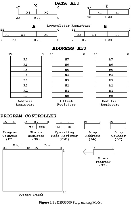
The 56000 is a 56-bit general purpose DSP chip which can execute 10.25 million instructions per second (MIPS). Its programming model consists of two 56-bit accumulators, ten data registers and a system stack. Figure 7.1 shows the programming model of the DSP. On the chip itself, there are two built-in independent 256 x 24-bit data RAMs (Random Access Memory) and two built-in independent 256 x 24-bit data ROMs (Read Only Memory). The off-chip memory expansion (i.e. additional RAM) can support 128k x 24-bit data memory and 64k x 24-bit program memory. Data memory is used for storing lookup tables & constants whereas program memory is used for storing the DSP56000 instructions.
The 56000 has three processing units operating in parallel : the data ALU, address ALU and program controller (ALU stands for arithmetic logic unit).
DATA ALU :
There are four 24-bit data registers X1, X0, Y1 and Y0. They can be treated either as four independent registers or as two 48-bit registers called X and Y. These registers are used as input pipeline registers between the X & Y data buses and the multiply-accumulator unit (MAC). This means that these registers are directly connected to the data buses and the MAC and they act as temporary storage. The MAC is a part of the data ALU of the 56000 that does multiplication and accumulation (i.e. add). The X and Y registers are also used as data ALU source operands and allow new operands to be loaded for the next instruction while the register contents are used by the current instruction.
There are six data ALU accumulator registers : A2, A1, A0, B2, B1 and B0. They may also be combined to form two general purpose 56-bit accumulators, A and B. These accumulators are used for arithmetic calculations and data manipulation.
The address ALU has three banks of registers : address registers (R0-R7), offset registers (N0-N7) and modifier registers (M0-M7). There are eight registers in each bank and each register is sixteen bits wide.
The contents of R0-R7 are used in the calculation of the effective address of an operand. Content modification of the address registers is controlled by the contents of the offset and modifier registers. These registers can also be used for general purpose storage.
The offset registers, N0-N7, contain offset values used to increment and decrement the address registers in address register update calculations or they can be used as general purpose storage. Each address register has its own offset register associated with it. For example, R0 is associated with N0, R1 with N1 and so on.
The contents of the eighth modifier registers, M0-M7, define the type of address arithmetic to be performed for address mode calculations and they can also be used as general purpose storage. Again, each address register has its own modifier register associated with it.
PROGRAM CONTROLLER :
The 16-bit program counter (PC) register holds the address of the next instruction to be fetched from the program memory space. The contents of the program counter are pushed into the stack when a program loop is started, when a jump to subroutine is performed, or when interrupts occur.
The status register (SR) has two parts, the mode register (MR) and the condition code register (CCR). The mode register is a special register that holds the current system state of the processor whereas the condition code register holds the current user state of the processor. Like the program counter, the status register is pushed into the stack when a program loop occurs, when a jump to subroutine is performed, or when interrupts occur.
The loop counter (LC) is used to specify the number of times to repeat a hardware program loop. The loop address (LA) register indicates the location of the last instruction word in a program loop. These registers are pushed into the stack when a DO instruction is encountered in the program and pulled out of the stack when an ENDDO instruction is encountered.
The System Stack (SS) is a separate internal memory which stores the program counter and the status register for subroutine calls and interrupts. It also stores the loop counter and loop address register in addition to the program counter and status register for program looping. The system stack is 32 bits wide and has 15 locations. When a subroutine call or interrupt occurs, the contents of the program counter and status register are stored (pushed) on the top of the location in the system stack. When a return from subroutine occurs, the contents of the top location in the system stack are transferred (pulled) to both the program counter and status register.
The DSP56000 has three groups of addressing modes [36] :
1.) Register Direct Modes :
Data or Control Register Direct
Address Register Direct
Address Modifier Register
Address Offset Register
2.) Address Register Indirect Modes :
No Update
Postincrement by 1
Postdecrement by 1
Postincrement by Offset Nn
Postdecrement by Offset Nn
Indexed by Offset Nn
Predecrement by 1
3.) Special Addressing Modes :
Immediate Data
Absolute Address
Immediate Short Data
Short Jump Address
Absolute Short Address
I/O Short Address
Implicit Reference
There are six types of instruction sets available for the DSP56000 [36] :
1.) Arithmetic Instructions
2.) Logical Instructions
3.) Bit Manipulation Instructions
4.) Loop Instructions
5.) Move Instructions
6.) Program Control Instructions
7.2 The Digidesign Sound Accelerator Card
The Sound Accelerator card (Photo 7.1 and Figure 7.2) is an integrated audio digital signal processing system for the Apple Macintosh computer. The Motorola DSP56000 just described is used as the card's digital signal processor.
The Nubus/host interface on the Sound Accelerator card is to be connected to the Macintosh computer so that the card can be controlled through it by the Macintosh.
The Sound Accelerator comes with 8k x 24-bit words of external data memory and 2k x 24-bit words of program memory. Upgrading to 16k, 32k, or 64k x 24-bit words of data memory and/or 8k or 32k x 24-bit words of program memory are also permitted. All the memory used are SRAM (static RAM) so that they are fast enough for the DSP56000 not to need to have wait states when accessing them.
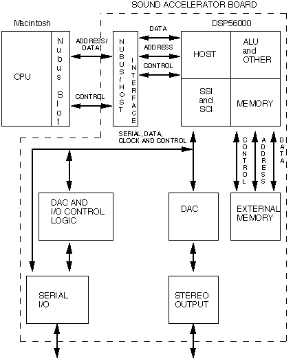
The card has a built in digital to analog (DAC) converter that can convert any processed digital data from the DSP56000 to analog signals to the outside world. It also has a serial digital input port (SERIAL I/O) for an external analog to digital (ADC) converter suitable for converting analog audio signals into digital data. The sampling rates of the ADC converter, when operating in stereo mode range from DC (0 Hz) to 156 kHz and when operating in mono range from DC to 312 kHz. The resolution of samples is at 16-bit. Higher sampling rates are possible when an external clock is used.
The DAC and I/O control logic controls the flow of data to the DACs, the clock speed of the ADCs, and control signal flow in and out of the serial I/O connector. Whether the clock of the ADC should come from an external device or from internally is controlled by this logic. It is also used to control the mode of audio, either stereo or mono.
The card comes with a standard set of MPW (Macintosh Programmer's Workshop) tools that can be used to program the DSP56000. MPW is the standard programming environment for the Macintosh series of computers. It is an integrated environment where all the commands and functions can be invoked by a few key strokes or mouse clicks. Additional functions, such as the tools for the DSP56000, can be added into the MPW environment and be called easily. The tools include the DSP56000 Assembler used for compiling the DSP56000 machine language, the DSP56000 Linker used for linking assembled machine language files with the various standard libraries and the DSP56000 Parser used for embedding the DSP56000 binary codes into an Apple Macintosh resource file ready to be loaded into the DSP56000 program memory. Subroutines and examples showing how to interfacing the Apple Macintosh computer to the Digidesign Sound Accelerator card are also included. These tools were used extensively in programming the Sound Accelerator Card.
Other tools that were available but not used in our experiments include the DSP56000 assembly language subroutines for performing Fast Fourier Transform (FFT) operations, digital filtering and other digital signal processing operations.
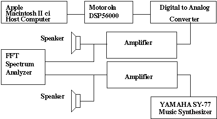
In figure 7.3, the setup of the real-time synthesis experiment is shown. The Apple Macintosh IIci host computer loads the machine code synthesis program into the Motorola DSP56000 and controls its states (i.e. execute, wait or stop). The DSP56000 runs either the AFM or DFM algorithm to synthesize the required musical instrument waveform. The output of the DSP56000 is then sent to the digital to analog converter on the Sound Accelerator Card and the resulting analog waveform amplified by an external amplifier. The amplified analog signal is then sent to the speaker for monitoring and the FFT spectrum analyzer for analysis. The original sampled waveform from the Yamaha SY77 synthesizer memory banks is also amplified and sent to the speaker and FFT spectrum analyzer for monitoring and analysis respectively, and for comparison with the AFM or DFM synthesized waveform.
The package of programs which implements the synthesis algorithm is in two parts : the control program for the host computer (an Apple Macintosh IIci computer) and the actual AFM or DFM synthesis program for the DSP56000. The control program, written in C (we used THINK C and MPW C for Apple Macintosh) [39][40], prepares the various parameters and sends them to the DSP56000 memory ready for reference by the DSP56000 program. It also controls the status of the DSP56000, i.e. makes it execute, wait or stop. The computational program does the actual real time synthesis by using the various parameters stored in the DSP56000 memory. It is written in Motorola DSP56000 assembly language (we used the Motorola DSP56000 Assembler and Linker). To change any of the synthesis parameters, we need only to change them in the control program which makes the task much easier. The listings of these DSP56000 assembly language programs and Think C programs are given in appendices 4, 5, 6, 7, 8, 9 and 10.
In the process of programming the DSP56000, several data memory locations of the DSP56000 must be reserved so that they could be used to store the various AFM or DFM parameters and also the starting and ending addresses of the lookup tables that would be loaded. The lookup tables include the sine lookup table, exponential lookup table (for AFM only), the amplitude envelope lookup table and the AFM or DFM parameters that we wanted to change in real-time during the synthesis.
On the Macintosh IIci, the control program written in THINK C language would load the various AFM or DFM parameters into the DSP56000 memory. The sine and exponential tables would be generated by the Macintosh IIci's 68030 and loaded into the predefined areas of the DSP56000 data memory. The amplitude envelope and the AFM or DFM parameters that we wanted to change in real-time during the synthesis would be defined manually by typing the values and sending them into the DSP56000 data memory.
The DSP56000 assembly programming was written in such a way that we could change the variable parameters of the synthesis algorithm (modulation index and ratio for the case of AFM and modulation indices for the case of DFM) at any point during the synthesis of a musical note. This was done by referring to the parameters stored as a table in the data memory of the DSP56000.
When the writing of the DSP56000 assembly program was completed, it was compiled, i.e. checked for programming errors and typing mistakes, and linked into a loadable file, i.e. a file that holds the actual binary codes readily understood by the DSP56000. The loadable file was then inserted into a resource file in the Macintosh IIci as part of its binary codes to be sent to the DSP56000 by the Macintosh interfacing program.
In summary, the programming procedure was as follows
1.) Reserve memory in DSP56000 for AFM or DFM parameters and lookup
tables.
2.) Load all synthesis parameters and lookup tables into the DSP56000 memory.
3.) Load compiled DSP56000 binary codes into DSP56000 and start the
synthesis process.
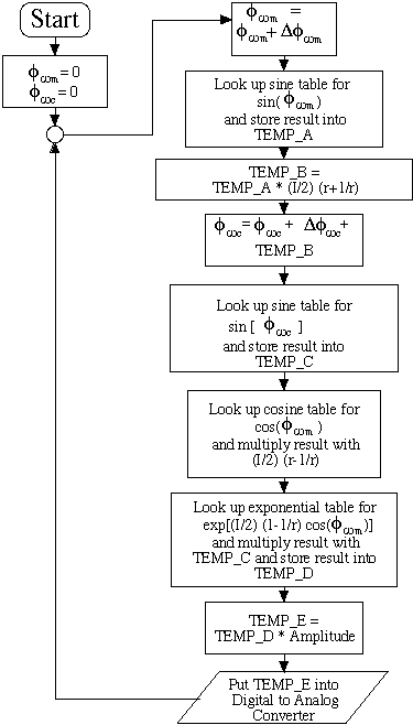
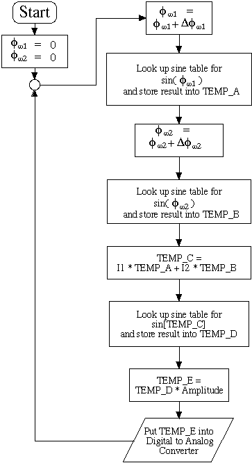
In figures 7.4 and 7.5, the algorithms for one AFM operator and one DFM operator are shown respectively in the form of flow charts. The following is a definition of the variables used in the flowcharts :
TEMP_A, TEMP_B, TEMP_C, TEMP_D and TEMP_E are variables declared for temporary storage of calculated intermediate values in the synthesis program.
For AFM,
[phi][omega]c = phase of carrier
[Delta][phi][omega]c = phase addition for carrier
[phi][omega]m = phase of modulator
[Delta][phi][omega]m = phase addition for modulator
For DFM,
[phi][omega]m1 = phase of modulator 1
[Delta][phi][omega]m = phase addition for modulator 1
[phi][omega]m2 = phase of modulator 2
[Delta][phi][omega]m = phase addition for modulator 2
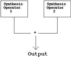
The various variables like [phi][omega]m, [phi][omega]c & TEMP_A for AFM and [phi][omega]m1, [phi][omega]m2 & TEMP_A for DFM are declared by having space reserved for them in memory locations in the DSP56000. The purpose of these phases are to simulate t (time) in the real time synthesis. This will be explained in the next section. For the case of two synthesis operators as in figure 7.6, another set of these phases are needed. Real time calculation of the second synthesis operator is done right after the first synthesis operator, i.e. in series. The results of all the synthesis operators are added and put into the digital to analog converter. After this, the whole process repeats until we stop it through the host computer.
7.3 The AFM Synthesis Program
For the AFM algorithm in figure 7.4, at the beginning of the program, the [phi][omega]m and [phi][omega]c have to be set to zero so that the phases of the carrier and modulator are zero at t = 0. Then [phi][omega]m is incremented with an addition of [Delta][phi][omega]m for each loop to represent the incremental passage of time [Delta]t. This is to be used as an argument for the sine function, i.e. sin([omega]mt).
For time t to increase at a constant rate, [phi][omega]m is to be increased at a constant rate. The result of the sine table look up, i.e. sin([omega]mt), is then stored temporarily in a buffer called TEMP_A. TEMP_A is then multiplied by (I/2) (r+1/r) and the result stored into TEMP_B. At this point, TEMP_B holds the calculated value of (I/2) (r+1/r) sin([omega]mt).
At the next step, [phi][omega]c is incremented by adding [Delta][phi][omega]c and TEMP_B. [phi][omega]c will thus hold another argument for the sine function, which is [omega]ct + (I/2) (r+1/r) sin([omega]mt). Another look up of the sine table is done and the result is stored into TEMP_C. TEMP_C will now hold the calculated value of sin[[omega]ct + (I/2) (r+1/r) sin([omega]mt)].
A look up for the value of cos([omega]mt) is then done and the result multiplied by (I/2) (r-1/r). Using the result of this multiplication, another look up for the exponential function is done, which is multiplied by the previous calculated value of sin[[omega]ct + (I/2) (r+1/r) sin([omega]mt)] stored in TEMP_C. The result is then stored in TEMP_D. The contents of TEMP_D are multiplied by the amplitude and stored into TEMP_E.
The temporary buffer TEMP_E now holds the value for A exp[(I/2) (1-1/r) cos([omega]mt)] (sin[[omega]ct + (I/2) (r+1/r) sin([omega]mt)], which is the AFM expression as in equation 3.10. This calculated value is then output to the digital to analog converter so that the analog voltage can be sent to the amplifier and speaker. The whole process then repeats itself to give another calculated value for the expression in equation 3.10 to be output to the digital to analog converter again.
7.4 The DFM Synthesis Program
The flowchart for the computation of the DFM algorithm is shown in figure 7.5. At the beginning, [phi][omega]m1 and [phi][omega]m2 are set to zero as for the AFM algorithm.
In the next step [phi][omega]m1 is incremented by adding [Delta][phi][omega]m1. This is made the argument for the sine function and a sine table look up is done with the result, i.e. sin([omega]m1t), stored in a temporary buffer TEMP_A. [phi][omega]m2 is then also incremented and similarly becomes an argument for another sine function. The sine table look up result for [phi][omega]m2 is then placed in a second buffer TEMP_B.
In the next stage, we multiply the contents of TEMP_A by [Iota]1 and the contents of TEMP_B by [Iota]2. The results of both multiplications are added and placed into TEMP_C.
At this point, TEMP_C now holds the calculated value for [Iota]1 sin([omega]m1t) + [Iota]2 sin([omega]m2t) which is made the argument for the sine function. After the sine table look up, the result is stored into TEMP_D. The contents of TEMP_D are then multiplied by the amplitude and the result stored into TEMP_E.
We thus have TEMP_E holding the calculated value for the equation A sin[[Iota]1 sin([omega]m1t) + [Iota]2 sin([omega]m2t)] which is the expression for DFM in equation 4.1. This is then output to the digital to analog converter to give an analog voltage. The whole process then repeats to give the next calculated value for the DFM expression in equation 4.1.
7.5 The "Do Nothing Loop"
After sending the various AFM or DFM parameters over to the DSP, the host computer loads the instructions into the DSP56000 memory and orders the DSP56000 to execute the codes in a loop, i.e. to run it over and over again. The speed with which the DSP56000 executes all the instructions in its memory is too fast and has to be slowed down so that the correct sound frequency is generated. This is achieved by the introduction of a "do nothing loop".
The "do nothing loop" consists of a few DSP56000 machine language instructions ordering the DSP56000 to run an instruction called "NOP" or No Operation for a given number of times. This will slow the DSP56000 down for a while before repeating all the instructions in the memory. The number of times the "do nothing loop" should execute is determined by first running the synthesis algorithm in the memory with a frequency setting of 1 kHz. The frequency of the output signal produced, which is higher than 1 kHz, is then measured by using a frequency counter or an oscilloscope. The relationship between the generated frequency, f, and number of times (n) added to some constant (k) (shown below) to execute the "do nothing loop" is inversely proportional for a synthesis algorithm as follows :
![]()
The correct value of n can thus be calculated given a desired value of f. The loop counter is then set to the correct value or n and the synthesis program is executed. The frequency of the generated waveform is checked again for minor adjustments to be made to the loop.
The loop index, i.e. the number of time the loop gets executed, depends on the clock speed of the DSP56000 (which is a constant) and the number of instructions the DSP56000 executes in its memory in one single run. Some instructions require only one clock cycle to execute and some require more clock cycles to complete. Generally, when the number of instructions to execute is increased, the number of times to execute the "do nothing loop" is decreased. After all these adjustments, the correctly calibrated DSP56000 can then generate the correct audio frequency.
7.6 Spectrum Analysis of Synthesized Sound
The DSP56000 synthesized waveform output from the D/A converter is sent to the FFT spectrum analyzer so that its spectrum can be compared with that of the sampled waveform. The comparisons are done by plotting the normalized spectra for the sampled waveform and the synthesized waveform together so that we can see which frequency components are different, i.e. higher or lower than the sampled ones. In the normalization of a spectrum, we have divided all the components by the amplitude of the maximum component for that spectrum.
7.7 Generation of Complete Sound
Earlier, we had divided each SY77 sample waveform into attack, attack-to-sustain and sustain portions for frequency analysis. This is to allow us to obtain the synthesis parameters (modulation index and ratio for AFM and modulation indices for DFM) for the attack, attack-to-sustain and sustain portions of the waveform.
We originally intended to change some of the synthesis parameters in real-time so as to achieve a dynamic spectrum, i.e. a spectrum which varies with time. However, we could not update the DSP memory from the host computer without stopping the DSP56000 from executing its program. A solution would be to place the parameters in sequence in the DSP56000 memory so that the DSP56000 can change the synthesis parameters in real-time during the synthesis of a musical note. The envelope function (i.e. attack, sustain and decay) of the particular instrument could also be stored in the memory of the DSP56000 to control the timbre of the sound generated.
With all the key parameters of the synthesis algorithm loaded into the DSP56000 memory, the DSP56000 could be made to execute the synthesis algorithm in real-time so that the entire waveform of a note of a musical instrument which has a dynamic spectrum can be synthesized.